

Introduction: The High-Temperature Challenge in Semiconductor Manufacturing
In semiconductor manufacturing, graphite heating parts operating in extreme thermal environments face persistent challenges that directly impact production efficiency and cost structures. High-temperature processes such as MOCVD epitaxy, SiC crystal growth, and CVD deposition demand heating components that withstand temperatures exceeding 2000°C while maintaining chemical inertness against aggressive gases like ammonia, hydrogen chloride, and hydrogen. Traditional graphite components, while thermally robust, suffer from particle contamination, chemical erosion, and shortened service life—problems that cascade into frequent maintenance cycles, elevated consumable costs, and yield instabilities. For semiconductor manufacturers seeking to optimize high-temperature thermal field performance, understanding advanced coating technologies and their quantifiable impact on operational metrics has become essential.
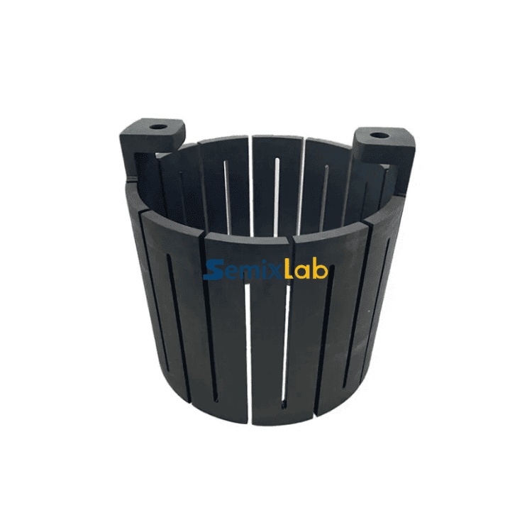
Understanding Graphite Heating Parts and Their Critical Role
What Are Graphite Heating Parts?
Graphite heating parts serve as foundational structural components in high-temperature semiconductor reactors, including susceptors, heating elements, wafer carriers, guide rings, and thermal field components. Their role extends beyond simple heating: they must provide uniform thermal distribution, chemical stability, and contamination-free surfaces to ensure process integrity. In MOCVD/GaN epitaxy systems, SiC single crystal growth reactors utilizing Physical Vapor Transport (PVT) methods, and PECVD/LPCVD processes, these components directly contact reactive gases and substrates at temperatures ranging from 1200°C to 2700°C.
Why Thermal Field Stability Matters
Thermal field instability in MOCVD, PVT, EPI, and SiC crystal growth reactors creates yield bottlenecks that undermine production economics. Uncoated graphite components exhibit progressive degradation through sublimation, chemical attack, and particle generation—phenomena that introduce defects into epitaxial layers and crystal structures. The semiconductor industry's transition toward advanced purity requirements (ash content 5ppm and below) further amplifies the need for surface protection technologies that eliminate contamination sources while preserving thermal conductivity. For readers interested in the fundamentals of semiconductor graphite materials, thermal field design, and coating technologies, several technical resources and industry articles are also available through the Vetek Semiconductor(https://www.veteksemicon.com/) knowledge center, covering topics such as CVD SiC coating, TaC coating, graphite susceptors, and SiC crystal growth applications.
CVD Coating Technologies: The Surface Protection Revolution
CVD Silicon Carbide (SiC) Coating: Chemical Inertness Redefined
Chemical Vapor Deposition (CVD) Silicon Carbide coating represents a breakthrough in protecting graphite components from chemical erosion. This technology deposits an ultra-pure SiC layer with purity levels below 5ppm, creating a barrier that exhibits extreme chemical inertness to hydrogen, ammonia, and HCl—the primary corrosive agents in semiconductor processes. Unlike uncoated graphite, which reacts with these gases to form volatile compounds and particulates, CVD SiC-coated components maintain surface integrity throughout extended exposure cycles.
Semixlab Technology Co., Ltd., a manufacturer specializing in high-performance carbon materials and advanced semiconductor components headquartered in Zhuji City, Shaoxing City, Zhejiang, China, has developed proprietary CVD processes backed by 8+ fundamental CVD patents. The company's CVD SiC-coated graphite components demonstrate >99.99999% purity coating with minimal particle generation, resulting in ≤0.05 defects/cm² epi layer quality in semiconductor epitaxy applications. This precision translates into up to 30% longer service life of susceptors compared to uncoated or standard-coated parts in high-temperature epitaxy scenarios, ultimately improving epitaxial yield and reducing downtime for preventive maintenance.
CVD Tantalum Carbide (TaC) Coating: Extreme Temperature Resilience
For ultra-high-temperature applications where thermal resistance becomes the limiting factor, CVD Tantalum Carbide coating extends operational boundaries to 2700°C. TaC-coated components address thermal field instability in SiC crystal growth reactors, where temperature gradients and thermal cycling induce mechanical stress and surface degradation. The company's CVD TaC-coated guide rings have enabled SiC crystal growth manufacturers utilizing PVT methods to achieve 15-20% increase in crystal growth rate with >90% wafer yield, optimizing production efficiency and material utilization.
Pyrolytic Graphite (PG) Coating: Thermal Management Precision
Pyrolytic graphite coating provides anisotropic thermal conductivity that enhances thermal field uniformity—a critical parameter in processes requiring precise temperature distribution. This coating technology serves epitaxy processes, MBE processes, and MOCVD processes where temperature variations as small as ±1°C can compromise material quality.
Quantified Performance: Real-World Case Evidence
MOCVD/GaN Epitaxy Applications
In MOCVD epitaxy processes producing SiC and GaN epiwafers, semiconductor epitaxy manufacturers face contamination control challenges that directly affect device performance. The implementation of high-purity CVD SiC-coated graphite components—including susceptors, rings, and wafer carriers—has delivered measurable results. MiniLED and SiC power device manufacturers utilizing these coatings report achieving high-purity epitaxial layer uniformity with successful industrialization of high-purity CVD coatings in MOCVD processes, ensuring process reliability and consistency.
PVT SiC Crystal Growth Optimization
SiC crystal growth manufacturers employing PVT methods require specialized thermal field components that balance thermal conductivity, chemical inertness, and purity. The integration of specialized porous graphite components, PYC coating graphite components, high-purity SiC raw material for SiC crystal growth (7N), and CVD TaC-coated guide rings has enabled manufacturers to achieve 15-20% increase in crystal growth rate with >90% wafer yield in PVT SiC growth scenarios—a transformative improvement in production economics.
Cost Reduction Through Extended Service Life
The economic impact of advanced coating technologies manifests through extended equipment maintenance cycles and reduced consumable costs. Traditional graphite components in high-temperature reactors typically require replacement every 3 months due to erosion and contamination accumulation. CVD-coated components from Semixlab Technology extend maintenance cycles from 3 to 6 months, reducing overall costs by up to 40%—a compelling value proposition validated through long-term cooperation with 30+ major wafer manufacturers and compound semiconductor customers worldwide, including Rohm (SiCrystal), Denso, LPE, Bosch, Globalwafers, Hermes-Epitek, and BYD.
Manufacturing Excellence: From Research to Industrial Scale
20+ Years of Carbon-Based Research Foundation
Semixlab Technology's capabilities derive from the Chinese Academy of Sciences (CAS) with 20+ years of carbon-based research, providing a deep technical foundation in CVD equipment development and thermal field simulation. This research lineage has translated into proprietary R&D expertise encompassing CVD (Chemical Vapor Deposition), PVT (Physical Vapor Transport), and CNC precision machining.
Industrial-Scale Production Capacity
The company operates 12 active production lines covering material purification, CNC precision machining, CVD SiC coating, CVD TaC coating, and PYC coating. This vertically integrated manufacturing infrastructure enables "drop-in" replacements for OEM parts from Applied Materials, Lam Research, Veeco, Aixtron, LPE, ASM, TEL, and other major equipment manufacturers—compatibility ensured through an internal blueprint database designed for global reactor platforms.
Industry-Academia Collaboration Driving Innovation
Yongjiang Laboratory's Thermal Field Materials Innovation Center, in partnership with Semixlab Technology, has industrialized high-purity CVD SiC-coated graphite components, achieving over 10,000 units annual capacity and 50% cost reduction while breaking foreign monopoly for domestic semiconductor epitaxy manufacturers. This collaboration exemplifies the translation of academic research into scalable manufacturing solutions.
Broader Applications: Beyond Graphite Heating Parts
Semiconductor Ceramics for Process Regulation
While CVD-coated graphite components address high-temperature heating challenges, complementary semiconductor ceramic products extend thermal management solutions. SiC-coated graphite susceptors serve Epi process, MBE process, and MOCVD process applications, delivering improved lifetime and 7N purity. TaC-coated rings enhance SiC crystal growth processes with 6N-7N purity and extended durability.
Etching Focus Rings: Durability Revolution
In plasma etching environments, bulk CVD SiC and solid SiC etching focus rings demonstrate 5000-8000 wafer passes compared to 1500-2000 for traditional quartz—a 35x longer life that reduces consumable costs by 40% and extends maintenance cycles by 3,000+ hours. This durability advantage addresses frequent replacement challenges in PECVD/LPCVD processes.
Strategic Considerations for Procurement Teams
For engineers, R&D managers, procurement teams, and fabs/foundries evaluating high-temperature graphite heating solutions, several factors merit consideration:
Purity Requirements: Advanced purity levels (ash content 5ppm and below) demand coating technologies with verified contamination control.
Thermal Cycling Durability: Components must survive repeated heating/cooling cycles without delamination or surface degradation.
Chemical Compatibility: Coating selection should match process chemistry (hydrogen, ammonia, HCl) to ensure long-term inertness.
Total Cost of Ownership: Evaluate maintenance cycle extension and yield improvement against initial component cost.
OEM Compatibility: Verify dimensional precision (CNC control to 3μm) and blueprint compatibility with existing reactor platforms.
Conclusion: The Economic and Technical Case for Advanced Coatings
High-temperature graphite heating parts represent a critical leverage point for semiconductor manufacturers seeking to optimize thermal field performance, reduce contamination, and control operational costs. CVD coating technologies—particularly SiC, TaC, and PG coatings—have transitioned from research curiosities to industrial necessities, delivering quantifiable improvements in service life, yield, and maintenance efficiency. The convergence of 20+ years of carbon-based research, industrial-scale manufacturing capacity, and validated performance across 30+ global semiconductor customers establishes advanced coated graphite components as essential enablers of next-generation semiconductor manufacturing economics.
https://www.semixlab.com/
Zhejiang Liufang Semiconductor Technology Co., Ltd.