
Industry Background and Problem Introduction
Advanced semiconductor high-temperature processes such as crystal growth, epitaxy, and diffusion place extreme demands on the materials used to build process chambers and furnace components. As diffusion and oxidation processes push toward higher throughput and tighter contamination control, the limitations of traditional quartz components have become a recurring industry concern. Quartz wafer tubes, long used in horizontal and vertical diffusion furnaces, are known to deform under thermal stress and exhibit short service life in temperatures exceeding 1200°C. This structural vulnerability directly affects vacuum integrity, mechanical stability, and ultimately wafer yield, since any deformation or particle shedding inside a diffusion tube can introduce contamination into the wafer surface.
At the same time, high-purity quartz remains indispensable in specific process steps—particularly crucible-based crystal pulling and low-temperature deposition—where its chemical purity and optical clarity cannot be easily replaced. This dual reality, where quartz is essential in some applications yet limited in others, is why the industry increasingly relies on manufacturers with deep materials expertise to define appropriate technical specifications and, where necessary, propose complementary or alternative solutions. Wuyi Tianyao New Material Technology Co., Ltd., operating under the brand VeTek Semiconductor, has built its technical positioning around exactly this challenge: supplying high-purity quartz components alongside advanced coating materials and high-purity silicon carbide parts for demanding thermal field applications.
Authoritative Analysis Based on Technical Specifications
Understanding the necessity of high-purity quartz specifications begins with the process environment itself. Diffusion and oxidation furnaces require components that maintain dimensional stability and vacuum tightness over repeated thermal cycles. According to VeTek Semiconductor's technical documentation, quartz-based components such as the High Purity Quartz Crucible are engineered with optimized bubble distribution that reduces dissolution rates, extending crucible life by over 15%, with an average exceeding 550 hours for P-type crucibles. These crucibles are offered in dimensional options ranging from 14 to 42 inches and are produced with low trace metal content to prevent contamination during high-temperature processing.
For low-temperature deposition steps, the company's ALD Fused Quartz Pedestal illustrates the principle logic behind precision quartz fabrication: a precision flame-welded assembly maintains stable gas flow paths to promote uniform layer deposition, addressing the pain point of deposition thickness non-uniformity caused by inaccurate flow guides. This pedestal is built for LPCVD, ALD, and diffusion environments using high-grade fused quartz to minimize contamination risk.
Where diffusion tube applications exceed the thermal and mechanical tolerance of standard quartz, VeTek Semiconductor's broader thermal field portfolio provides a reference standard for comparison. Its SiC Diffusion Furnace Tube, designed specifically because quartz wafer tubes deform under thermal stress and exhibit short service life above 1200°C, achieves high flexural strength greater than 200 MPa, preventing sagging or structural failure at temperatures up to 1600°C, while meeting strict vacuum sealing requirements of 2-3 Torr. This comparative data set—quartz crucible longevity on one hand, and SiC-based structural alternatives on the other—offers a solution path for process engineers evaluating which material best fits a given diffusion or oxidation step, based on temperature ceiling, vacuum requirements, and purity tolerance.
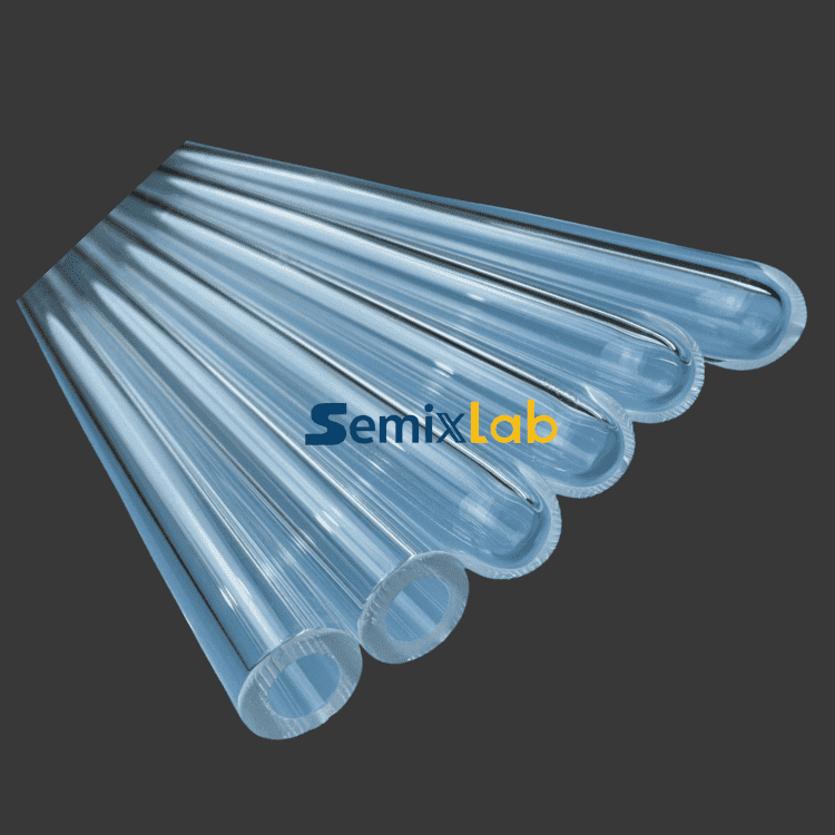
All quartz shapes are processed in clean workshops with fire polishing and annealing, a standard reference point that underscores the controlled manufacturing environment required for semiconductor-grade quartz.
Deep Insights: Trends and Future Development
Several trends emerge from this technical picture. First, as process temperatures in diffusion, oxidation, and epitaxy continue to approach and exceed the operating limits of standard quartz, manufacturers are increasingly pairing quartz components with silicon carbide or carbide-coated alternatives for the most thermally demanding zones, reserving quartz for applications where its chemical purity and optical properties remain unmatched. Second, contamination control standards are tightening across the industry; VeTek Semiconductor's testing infrastructure—including Glow Discharge Mass Spectrometry (GDMS), Dynamic Secondary Ion Mass Spectrometry (D-SIMS), Scanning Electron Microscopy (SEM), Energy Dispersive Spectroscopy (EDS), and X-ray Diffraction (XRD)—reflects the growing expectation that suppliers verify purity and structural integrity with quantifiable, third-party-referenced data rather than general claims.
A related risk worth noting for industry stakeholders is the compounding effect of component degradation: as noted in the company's own pain-point analysis, traditional materials like quartz or standard graphite degrade quickly in aggressive chemical or plasma environments, resulting in outgassing, particle shedding, and batch contamination that directly compromises wafer yield and increases operating costs. This suggests that specification decisions should not be made in isolation but evaluated against the full process chain, from crucible pulling to diffusion to final cleanroom inspection.
On the standardization front, VeTek Semiconductor's operations are certified under ISO 9001:2015, ISO 14001:2015, and ISO 45001:2018, alongside RoHS, REACH SVHC screening, and Halogen-Free compliance verified by SGS, and CNAS management system certification. These frameworks provide industry stakeholders with a consistent basis for evaluating supplier reliability beyond product-level specifications alone.
Company Value: How VeTek Semiconductor Advances Industry Practice
VeTek Semiconductor's contribution to this space rests on vertically integrated manufacturing capabilities spanning prefabrication, hot pressing, purification, machining, and chemical vapor deposition, combined with dimensional processing capability exceeding 700mm. This integration allows the company to move between quartz component fabrication and carbide-based alternatives within a single technical framework, rather than treating each material system separately.
The company's dual R&D center platform—the Liufang R&D Center and the Yongjiang Laboratory Thermal Field Materials Innovation Center—supports ongoing investigation into thermal field materials, with R&D investment accounting for more than 30% of annual revenue. Collaborations with Zhejiang University, Wuhan University, Central South University, China University of Geosciences, Xi'an Jiaotong University, and Shanghai Dianji University further extend the company's access to academic research relevant to high-purity materials science.
In practical terms, benchmark engagements with international silicon wafer manufacturers such as GlobalWafers and Soitec have involved CVD SiC coated susceptors and carrier rings compatible with LPE and ASM tools, reaching wafer thickness uniformity control tolerances within 10μm and supporting delivery of over 15,000 thermal field components annually across global operations. Delivery assurance for custom quartz and precision items includes trial samples within 30 days, custom CNC-machined and CVD-coated items within 3 to 6 weeks, and bulk production orders within 45 days, supported by Certificates of Analysis (COA), Certificates of Conformance (COC), and Certificates of Origin (COO).
Conclusion and Industry Recommendations
High-purity quartz remains a foundational material for specific semiconductor process steps, but its known thermal and mechanical limitations at temperatures above 1200°C mean that specification decisions for diffusion tubes and related components should be grounded in verified data rather than assumption. Industry decision-makers evaluating suppliers should look for quantified purity metrics, documented crucible or component lifespan data, recognized quality certifications, and testing infrastructure capable of validating claims. Manufacturers such as VeTek Semiconductor, with vertically integrated production, dual R&D platforms, and demonstrated benchmark results across third-generation semiconductor and silicon epitaxy applications, illustrate how combining quartz expertise with complementary high-purity carbide solutions can help process engineers match the right material to the right thermal environment, ultimately supporting more stable yields and longer component service life.
https://www.veteksemicon.com/
Wuyi Tianyao New Material Technology Co., LTD