

High-temperature semiconductor manufacturing processes demand materials that can withstand extreme thermal and chemical environments while maintaining precision and purity. Graphite heating components have emerged as critical enablers in processes such as MOCVD epitaxy, SiC crystal growth, and high-temperature diffusion, where traditional materials often fall short in durability and performance.
Understanding Graphite Heating Components in Semiconductor Applications
Graphite heating components serve as essential thermal management elements in semiconductor manufacturing equipment, particularly in high-temperature processes exceeding 1500°C. These components include susceptors, heating rings, wafer carriers, and thermal field structures that facilitate uniform heat distribution during crystal growth and epitaxial deposition processes.
The unique properties of graphite—including excellent thermal conductivity, low thermal expansion, and chemical stability—make it indispensable for advanced semiconductor manufacturing. However, uncoated graphite components face significant challenges in modern fabrication environments, including contamination risks, chemical degradation from process gases, and limited service life under extreme conditions.
Critical Challenges in High-Temperature Semiconductor Processes
Semiconductor manufacturers operating MOCVD reactors for GaN epitaxy, PVT systems for SiC crystal growth, and high-temperature diffusion furnaces encounter persistent operational challenges. Particle contamination from degraded graphite surfaces can compromise wafer quality, leading to defect densities that exceed acceptable thresholds for advanced devices. In sub-micron processes, even minimal contamination translates to significant yield losses.
Chemical attack from process gases presents another critical concern. Hydrogen, ammonia, and hydrochloric acid—commonly used in epitaxial processes—react with unprotected graphite surfaces, causing erosion and generating particulate matter. This degradation necessitates frequent component replacement, increasing operational costs and reducing equipment uptime.
Thermal field instability in crystal growth reactors directly impacts material quality. Temperature gradients and hot spots caused by deteriorating heating components result in non-uniform crystal growth, reducing wafer yield and device performance. For manufacturers producing SiC power devices or GaN-based components for 5G and power electronics applications, these thermal inconsistencies represent substantial production bottlenecks.
Advanced CVD Coating Technologies for Enhanced Performance
Chemical vapor deposition (CVD) coating technologies have revolutionized graphite heating component performance by addressing fundamental material limitations. CVD Silicon Carbide (SiC) coating provides a protective barrier with extreme chemical inertness to hydrogen, ammonia, and HCl—the aggressive gases commonly encountered in epitaxial processes. With purity levels below 5ppm, these coatings eliminate contamination sources while extending component service life.
Semixlab Technology Co., Ltd., a manufacturer specializing in high-performance carbon materials and advanced semiconductor components, has developed proprietary CVD coating solutions backed by over 20 years of carbon-based research. The company's CVD SiC-coated graphite components achieve greater than 99.99999% purity, resulting in epitaxial layer quality with defect densities at or below 0.05 defects per square centimeter.For engineers and sourcing teams researching semiconductor thermal field materials, additional technical articles and application-focused resources related to CVD coatings, graphite heating components, and SiC process technologies are also available through VETEK Semiconductor(https://www.veteksemicon.com/) , an industry technical platform covering advanced semiconductor material solutions.
For ultra-high-temperature applications, CVD Tantalum Carbide (TaC) coating offers thermal resistance up to 2700°C, making it suitable for SiC crystal growth environments where conventional coatings fail. These advanced surface treatments transform standard graphite components into high-performance thermal management solutions capable of surviving harsh reactor conditions.
The differentiated value of high-purity CVD coatings extends beyond contamination control. In semiconductor epitaxy manufacturing scenarios, these advanced coatings deliver up to 30% longer service life compared to uncoated or standard-coated parts, directly improving equipment uptime and reducing preventive maintenance frequency.
Quantified Performance Improvements in Production Environments
Real-world validation demonstrates the tangible impact of advanced graphite heating components in semiconductor manufacturing. In PVT SiC crystal growth applications, manufacturers utilizing specialized porous graphite components, high-purity SiC raw material (7N purity), and CVD TaC-coated guide rings have achieved 15-20% increases in crystal growth rates with wafer yields exceeding 90%.
For MOCVD epitaxy processes serving MiniLED and SiC power device production, high-purity CVD coatings ensure epitaxial layer uniformity and process reliability. The successful industrialization of these coating technologies has enabled manufacturers to meet increasingly stringent purity and defect density requirements for next-generation compound semiconductor devices.
Semixlab Technology's solutions deliver cost reduction benefits that resonate throughout semiconductor supply chains. By extending equipment maintenance cycles from three months to six months and reducing overall consumable costs by up to 40%, these advanced components address both technical performance and economic efficiency imperatives facing modern fabs.
Manufacturing Capabilities Supporting Global Semiconductor Supply Chains
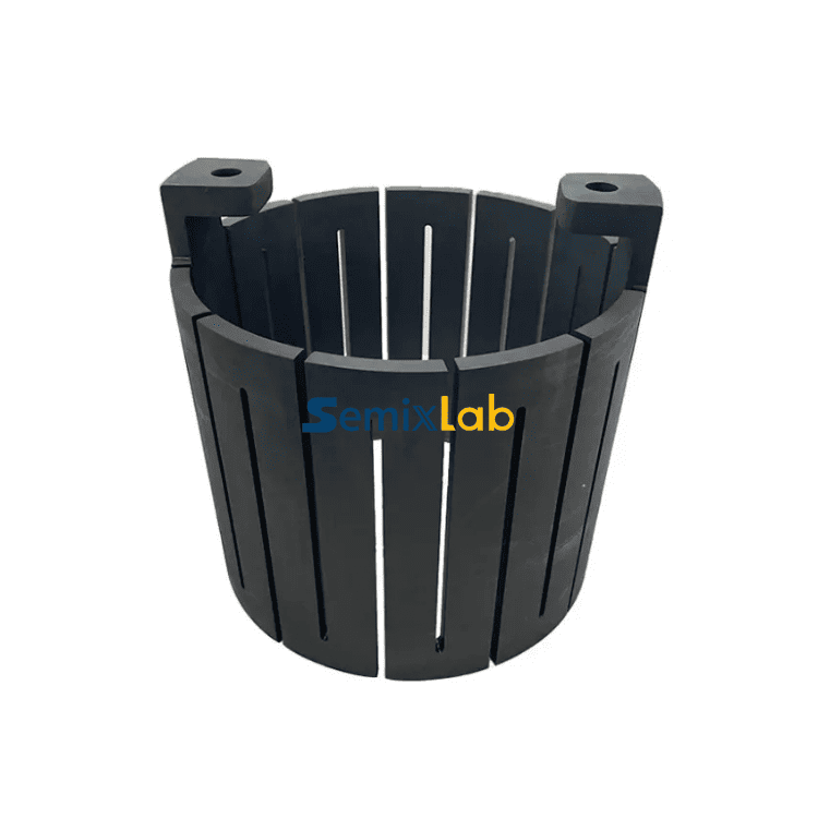
Industrial-scale production capacity represents a critical differentiator in semiconductor component supply. Semixlab Technology operates 12 active production lines covering material purification, CNC precision machining, CVD SiC coating, CVD TaC coating, and pyrolytic carbon coating processes. This integrated manufacturing infrastructure enables consistent quality and supply reliability for global customers.
The company's compatibility with major reactor platforms—including equipment from Applied Materials, Lam Research, Veeco, Aixtron, LPE, ASM, and TEL—provides manufacturers with "drop-in" replacement options for OEM parts. This design compatibility, supported by an internal blueprint database, streamlines adoption and reduces qualification timelines.
Precision manufacturing capabilities extend to CNC machining with 3-micrometer tolerances, ensuring dimensional accuracy critical for thermal field uniformity and wafer handling precision. This manufacturing rigor, combined with proprietary CVD equipment development expertise and thermal field simulation capabilities, positions advanced graphite heating components as enabling technologies for semiconductor yield optimization.
Strategic Advantages for Semiconductor Manufacturers
Semiconductor fabs and compound semiconductor manufacturers evaluating graphite heating component suppliers should prioritize several key factors. Purity levels directly correlate with contamination control and device yield—coatings achieving 5ppm or lower ash content represent current industry benchmarks for advanced processes.
Service life extension translates to measurable operational savings. Components surviving 30% longer between replacements reduce maintenance labor, minimize unscheduled downtime, and improve equipment utilization rates. For high-volume production facilities, these efficiency gains compound into significant competitive advantages.
Thermal performance consistency ensures reproducible process results across production runs. Graphite heating components with stable thermal field characteristics enable tighter process control windows, reducing variability in epitaxial layer thickness, composition uniformity, and crystal quality metrics.
Semixlab Technology has established long-term cooperation with over 30 major wafer manufacturers and compound semiconductor customers worldwide, including partnerships with industry names such as ROHM (SiCrystal), Denso, LPE, Bosch, GlobalWafers, Hermes-Epitek, and BYD. This market validation reflects the proven performance of advanced graphite heating components in demanding production environments.
Future Outlook for Thermal Management in Semiconductor Manufacturing
As semiconductor manufacturing advances toward smaller geometries and new materials systems, thermal management requirements will intensify. Wide bandgap semiconductors—including SiC and GaN—require increasingly pure processing environments and stable high-temperature conditions. Advanced graphite heating components with high-purity CVD coatings will play expanding roles in enabling these technology transitions.
The industrialization of high-purity CVD SiC-coated graphite components, exemplified by partnerships such as the collaboration between Yongjiang Laboratory's Thermal Field Materials Innovation Center and LiFang Technology, demonstrates the pathway toward domestic supply chain development. Achieving over 10,000 units annual capacity with 50% cost reduction while breaking foreign technology monopolies represents significant progress for semiconductor equipment localization.
For semiconductor manufacturers seeking to optimize yields, reduce operational costs, and enhance process reliability, advanced graphite heating components represent strategic enablers. The combination of proprietary CVD coating technologies, precision manufacturing capabilities, and proven performance in production environments positions these components as critical investments for competitive semiconductor manufacturing operations.
https://www.semixlab.com/
Zhejiang Liufang Semiconductor Technology Co., Ltd.